What’s inside the Snapdragon 855? – Gary Explains [Video]
Video uploaded by Android Authority on December 5, 2018
What is the 7nm Process and How It Will Change Our Gadgets?
Last November the IT community was discussing the 7nm process CPUs for the top iPads Pro with Face ID that are to arrive in 2018. The Taiwan Semiconductor Manufacturing Company or TSMC reportedly launched a product line to meet the demand in the new Apple tablets that are anticipated this year.
These iPads are rumored to feature the new A11X Bionic system-on-chip – which is considered the fastest and the slimmest of all mobile CPUs so far. The words “7nm process” are buzzing everywhere… in reviews, articles, blogs and Facebook posts. For most of the people who work outside of the IT business this phrase probably sounds like gibberish, but not to worry… iGotOffer will tell you everything about the 7nm process you didn’t know and were afraid to ask!
As you know from our “CPU for Dummies” article a CPU is an office building packed with tiny but very hardworking clerks-transistors. These clerks are becoming smaller with every next generation to meet the industry demands.
But how does this ‘office building’ look in reality? Surprisingly, it looks very much like a wafer cake. It is even called the same. But in terms of CPU manufacturing, the wafer is baked not from flour and butter but from silicon. Then the laser beam print the transistors on these wafers the same way you can draw various figures with frosting when you’re decorating your cake.
The thickness of the laser beam is very critical. The thinner is the beam, the smaller the transistors are and then more of them can be placed on a wafer. When we talk about nanometer processes we talk about the thickness of this very beam. Obviously, we need our clerks to be as miniscule as possible. The smaller transistor is cooler and more power efficient than its’ bigger counterpart. Technically, we can achieve that. We can print transistors with the laser beam that is 7nm thick and even 5nm and 1nm. The problem is, these transistors won’t work because they will be short-circuited if powered. Why so? Because working within the 7nm and 5 nm scale we go to the sub-atomic level. Yes, S-U-B – A-T-O-M-I-C.

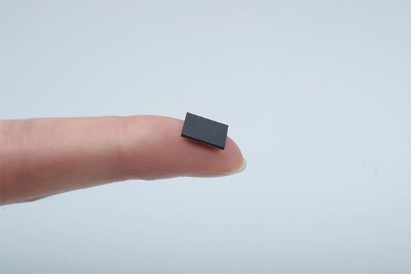
World’s first 7nm SoC Qualcomm Snapdragon 855
As you know, every atom consists of elementary particles, the biggest of them are electrons that orbit around the nucleus. Once the atom’s integrity is destroyed, they easily evaporate. Every free electron can short-circuit the system very quickly. This problem hasn’t been solved yet, scientists haven’t discovered or developed a material that is stable enough to survive the 5nm process without the electrons losing their tracks.
And yet, the TSMC announced that it has launched the 7nm process and is printing the next generation of CPUs. It’s a well-known and trusted company that has been working with Apple Inc. since iPads Pro powered by 10nm A10 chips. How could it be that a Taiwan company took the upper hand over Intel and Samsung that were working hard over diminishing the technological process? This is where we’re leaving the realm of technologies and entering the marketing world.
Let me repeat it again: the technical process is determined by the laser beam thickness. But marketing experts are talking about the size of a transistor itself. Can you see the difference? The thickness of the beam is not equal to the size of transistors it prints. To get more space and to increase the transistors efficiency the manufacturers changed the transistor’s design. This change took place quite a long time ago, back in 2001. I won’t get further into technical details, as I’m writing for average users like myself. It’s safe to say that these modified ‘clerks’ are the Olympic athletes in the world of transistors. They are slim, fast and strong. They can also be diminished down to 7 nm without their abilities being crippled in any way.
Many experts take this news with a grain of salt and point out that while talking about 10nm chips, what companies really mean is the 22nm process. And with the 7nm process we deal with the 14nm in the very best. What does it mean for us? Nothing. The new chips are going to be faster and cooler (in both senses of this word) than their predecessors. They just won’t be as cool as the manufacturers want them to be. If you ask me, the problem is not in the size of the hardware but in the software optimization. My laptop is one hundred times more powerful than the desktop I owned in 1998, but Office Word is freezing the same way it used to back then. Let’s optimize what we already have on our hands right now.
P.S. In February, 2018, TSMC started constructing the 5nm fab. The test run is scheduled for 2019, and the mass production – for 2020.
Links
- A-series chip supplier TSMC working on making 5nm chips in 2020, 3nm in 2022 – 9to5Mac.
- Thinking to sell your old cell phone? iGotOffer is the best place to sell smartphones and other electronic devices online.
- Everything About Apple’s Products – The complete guide to all Apple consumer electronic products, including technical specifications, identifiers and other valuable information.
- Everything About Microsoft’s Products – The complete guide to all Microsoft consumer electronic products, including technical specifications, identifiers and other valuable information.


Facebook
Twitter
RSS